- 您现在的位置:买卖IC网 > Sheet目录287 > 24LC64XT-I/ST (Microchip Technology)IC SERIAL EEPROM 64K 2.5V 8TSSOP
�� �
�
�24AA64/24LC64�
�3.6�
�Device� Addressing�
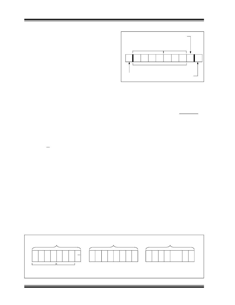
�FIGURE� 3-2:�
�CONTROL� BYTE� FORMAT�
�A� control� byte� is� the� first� byte� received� following� the�
�START� condition� from� the� master� device� (Figure� 3-2).�
�The� control� byte� consists� of� a� four� bit� control� code;� for�
�Read/Write� Bit�
�Chip� Select�
�the� 24XX64� this� is� set� as� 1010� binary� for� read� and� write�
�operations.� The� next� three� bits� of� the� control� byte� are�
�Control� Code�
�Bits�
�the� chip� select� bits� (A2,� A1,� A0).� The� chip� select� bits�
�S�
�1�
�0�
�1�
�0�
�A2�
�A1�
�A0� R/W� ACK�
�allow� the� use� of� up� to� eight� 24XX64� devices� on� the�
�same� bus� and� are� used� to� select� which� device� is�
�accessed.� The� chip� select� bits� in� the� control� byte� must�
�Slave� Address�
�correspond� to� the� logic� levels� on� the� corresponding� A2,�
�A1,� and� A0� pins� for� the� device� to� respond.� These� bits�
�are� in� effect� the� three� Most� Significant� bits� of� the� word�
�START� Bit�
�Acknowledge� Bit�
�address.�
�3.7�
�Contiguous� Addressing� Across�
�The� last� bit� of� the� control� byte� defines� the� operation� to�
�be� performed.� When� set� to� a� one� a� read� operation� is�
�selected,� and� when� set� to� a� zero� a� write� operation� is�
�selected.� The� next� two� bytes� received� define� the�
�address� of� the� first� data� byte� (Figure� 3-3).� Because�
�only� A12...A0� are� used,� the� upper� three� address� bits�
�are� don’t� care� bits.� The� upper� address� bits� are� trans-�
�ferred� first,� followed� by� the� less� significant� bits.�
�Following� the� START� condition,� the� 24XX64� monitors�
�the� SDA� bus� checking� the� device� type� identifier� being�
�transmitted.� Upon� receiving� a� 1010� code� and� appropri-�
�ate� device� select� bits,� the� slave� device� outputs� an�
�Acknowledge� signal� on� the� SDA� line.� Depending� on� the�
�state� of� the� R/W� bit,� the� 24XX64� will� select� a� read� or�
�write� operation.�
�Multiple� Devices�
�The� chip� select� bits� A2,� A1,� A0� can� be� used� to� expand�
�the� contiguous� address� space� for� up� to� 512K� bits� by�
�adding� up� to� eight� 24XX64's� on� the� same� bus.� In� this�
�case,� software� can� use� A0� of� the� control byte� as�
�address� bit� A13,� A1� as� address� bit� A14,� and� A2� as�
�address� bit� A15.� It� is� not� possible� to� sequentially� read�
�across� device� boundaries.�
�FIGURE� 3-3:�
�ADDRESS� SEQUENCE� BIT� ASSIGNMENTS�
�CONTROL� BYTE�
�ADDRESS� HIGH� BYTE�
�ADDRESS� LOW� BYTE�
�0� R/W�
�1�
�0�
�1�
�0�
�A�
�2�
�A�
�1�
�A�
�X�
�X�
�X�
�A� A� A�
�12� 11� 10�
�A�
�9�
�A�
�8�
�A�
�7�
�?�
�?�
�?�
�?�
�?�
�?�
�A�
�0�
�CONTROL�
�CODE�
�DS21189F-page� 6�
�CHIP�
�SELECT�
�BITS�
�X� =� Don’t� Care� Bit�
�?� 2002� Microchip� Technology� Inc.�
�发布紧急采购,3分钟左右您将得到回复。
相关PDF资料
24LCS21A/P
IC EEPROM 1KBIT 400KHZ 8DIP
24LCS22A-I/P
IC EEPROM 2KBIT 400KHZ 8DIP
24VL014/SN
IC EEPROM 1KBIT 400KHZ 8SOIC
24VL014H/SN
IC EEPROM 1KBIT 400KHZ 8SOIC
24VL024/SN
IC EEPROM 2KBIT 400KHZ 8SOIC
24VL024H/SN
IC EEPROM 2KBIT 400KHZ 8SOIC
25A512-I/ST
IC EEPROM 512K SPI BUS 8TSSOP
25AA020A-I/MS
IC EEPROM 2KBIT 10MHZ 8MSOP
相关代理商/技术参数
24LC65/P
功能描述:电可擦除可编程只读存储器 8kx8 2.5V Smart RoHS:否 制造商:Atmel 存储容量:2 Kbit 组织:256 B x 8 数据保留:100 yr 最大时钟频率:1000 KHz 最大工作电流:6 uA 工作电源电压:1.7 V to 5.5 V 最大工作温度:+ 85 C 安装风格:SMD/SMT 封装 / 箱体:SOIC-8
24LC65/P
制造商:Microchip Technology Inc 功能描述:IC EEPROM SMART SERIAL 64K 24LC65
24LC65/PG
功能描述:电可擦除可编程只读存储器 8kx8 - 2.5V Smart Lead Free Package
RoHS:否 制造商:Atmel 存储容量:2 Kbit 组织:256 B x 8 数据保留:100 yr 最大时钟频率:1000 KHz 最大工作电流:6 uA 工作电源电压:1.7 V to 5.5 V 最大工作温度:+ 85 C 安装风格:SMD/SMT 封装 / 箱体:SOIC-8
24LC65/SM
功能描述:电可擦除可编程只读存储器 8kx8 2.5V Smart RoHS:否 制造商:Atmel 存储容量:2 Kbit 组织:256 B x 8 数据保留:100 yr 最大时钟频率:1000 KHz 最大工作电流:6 uA 工作电源电压:1.7 V to 5.5 V 最大工作温度:+ 85 C 安装风格:SMD/SMT 封装 / 箱体:SOIC-8
24LC65/SM
制造商:Microchip Technology Inc 功能描述:IC EEPROM SMART SERIAL 64K 24LC65
24LC65/SMG
功能描述:电可擦除可编程只读存储器 8kx8 - 2.5V Smart Lead Free Package
RoHS:否 制造商:Atmel 存储容量:2 Kbit 组织:256 B x 8 数据保留:100 yr 最大时钟频率:1000 KHz 最大工作电流:6 uA 工作电源电压:1.7 V to 5.5 V 最大工作温度:+ 85 C 安装风格:SMD/SMT 封装 / 箱体:SOIC-8
24LC65-I/P
功能描述:电可擦除可编程只读存储器 8kx8 - 2.5V Smart RoHS:否 制造商:Atmel 存储容量:2 Kbit 组织:256 B x 8 数据保留:100 yr 最大时钟频率:1000 KHz 最大工作电流:6 uA 工作电源电压:1.7 V to 5.5 V 最大工作温度:+ 85 C 安装风格:SMD/SMT 封装 / 箱体:SOIC-8
24LC65-I/P
制造商:Microchip Technology Inc 功能描述:IC EEPROM SMART SERIAL 64K 24LC65